
| Home Page | Overview | Site Map | Index | Appendix | Illustration | About | Contact | Update | FAQ |
 |
 |
implies atomic and molecular sizes or smaller. Recently, research in the intermediate (mesoscopic) domain has achieved significant scientific successes. This field is characterized by the need to use the microscopic laws of quantum mechanics, while, on the other hand, the samples can be made and operated by essentially ordinary macroscopic methods. This involves linear size scales from a few to thousands of atoms, and reliable fabrication and analysis methods exist down to the scale of about fifty atoms. The term "nano" usually denotes the low end of this range. |
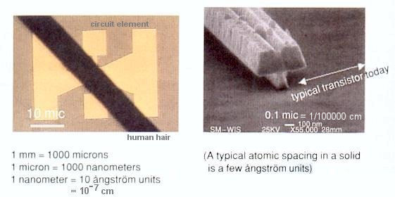
Figure 12-36a Nano Domain [view large image] |
Figure 12-36b Nanowires |
Figure 12-36a shows (left) scale of 10 micron with a circuit board element comparing to a human hair, and (right) 0.1 micron, where a small stat-of-the-art transistor is compared with one commercially available in 2001. Different types of nanowires are shown in Figure 12-36b, the insert in that image compares the size with blood cell. |
 |
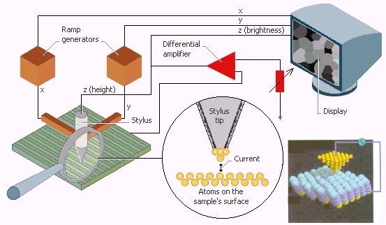
Methods based on extremely powerful scanning tunneling microscope (STM, Figure 12-36c) that allows control of both fabrication and analysis on the scale of single atoms are being developed. Controlling man-made molecular structures on the level of individual atoms (including position and orientation) is possible in principle, and physical measurements such as that of the local (atomic scale) density of electronic states near an appropriate defect in a superconductor have been made. A variety of surface probes can measure, for example, the local electrostatic potential on a sample's surface with a resolution approaching 10 nm. |
Figure 12-36c STM |
 |
There are two distinct approaches to manufacture small-scale devices. Microelectronics starts with a large system and then divides it, reducing its dimensions by a variety of well-controlled methods. For example, shapes are printed onto the surface of silicon, which is then etched away to make microscopic wheels or micromotors. The smallest feature capability that can be achieved, appear to be around the 10 nm scale. Other methods work with individual atoms to make even smaller objects. An example of such large-scale preparation of high-quality materials is provided by the MBE (molecular-beam-epitaxy) method (Figure 12-36d), which can be used to grow individual lattice layers and extra-thin metallic layers. |
Figure 12-36d MBE |
 |
The graphite phase of carbon provides some interesting nano materials such as carbon nanotubes and buckyballs (Figrure 13-36d). Nanotubes are produced by rolling a layer of two-dimensional graphite, called graphene, into a hollow cylinder parallel to the z axis and having a nanmeter-scale diameter. Graphene is a poor conductor, but the nanotube becomes metallic or semiconducting depending on the details of how exactly the graphene sheet is wound and connected to itself. Spherical fullerene (buckyball) contains 60 or 70 carbon atoms in the soccerball-like crystal of about 1 nm across. As of the early 21st century, the chemical and physical properties of fullerenes are still under heavy study. Fullerenes are not very reactive due to the stability of the graphite-like bonds, and are also sparingly soluble in many solvents. The buckyball has been used to run tests on determining the boundary between classical and quantum domains since its size is close to the transitional zone. Scientists are also working on building very small structures such as the nanorobot (Figure 12-36e), which can check out a patient's blood cells. The microgears were made by etching silicon in the same way as a microchip. Sixty of them would fit on the head of a pin. |
Figure 12-36e Nano Objects |
See more detailed and updated info on "Graphene". |