
| Home Page | Overview | Site Map | Index | Appendix | Illustration | About | Contact | Update | FAQ |
|
The first powerful magnifier was probably made by Anthony Leeuwenhoek (1632-1723) while working with magnifying glasses in a dry goods store. He used the magnifying glass to count threads in woven cloth. He became so interested that he learned how to make lenses. By grinding and polishing, he was able to make small lenses with great curvatures. These rounder lenses produced greater magnification, and his microscopes were able to magnify up to 270X. Because it had only one lens, Leeuwenhoek's microscope is now referred to as a single-lens microscope. Its convex glass lens was attached to a metal holder and was focused using screws. With such microscope, he discovered microorganisms - bacteria, yeast, blood cells and many tiny animals swimming about in a drop of water - thereby founding the science of microbiology and providing the basis for the development of the germ theory of disease. From his great contributions, many discoveries and research papers, Anthony Leeuwenhoek has since been called the "Father of Microscopy". |
Figure 1 Anthony van Leeuwenhoek[view large image] |
 = (h/f)/(h/25)
  -------------------- (1).
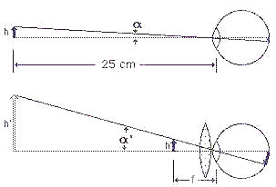 |
This formula is applicable when the virtual image h' is at infinity by placing the object at the focal point. Thus the object distance is the focal length f. The formula shows that lens with shorter focal length (greater curvature) yields more magnifying power. You can get a bit more magnification from the magnifier by focusing it so that the virtual image is at 25 cm rather than infinity, but it is not a good idea because it puts the eye of the viewer under strain to accommodate the image in that close distance. The relaxed eye is focused at infinity, so if you are going to use a microscope all day, you had better focus it at infinity. |
Figure 2a Magnifier |
 |
the light rays spread more, so that they appear to come from a large inverted image beyond the object lens. Because light rays do not actually pass through this location, the image is called a virtual image. The linear magnification or transverse magnification is the ratio of the image size to the object size. If the image and object are in the same medium it is just the negative of the image distance L + fo divided by the object distance fo (by basic trigonometry, see Figure 2b). The commonly stated expressions for microscope magnification are |
Figure 2b Compound Microscope [view large image] |
based on the assumption that the length of the tube L is large compared to either fo or fe so that the following relationships hold (the negative sign denotes inverted or virtual image) : |
 - L / fo ---------- (2).
 = - (L/fo)(25/fe) ---------- (3).
 ) / (n x sinA) --------------------- (4), is the wavelength of the energy source, n is the index of refraction of the lens, and A is the aperture angle2.
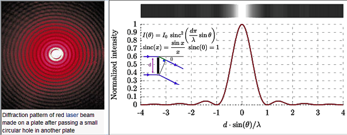 |
 |
A technology called structured illuminartion microscopy (SIM) can improve the resolution to about 10-5 cm with the cells tagged with fluorescent dyes. An image of microtubules in an epithelial cell from SIM is shown in Figure 3b (microtubules in red, DNA in blue, and the anchoring protein structures in green). The next challenge is to obtain unlimited resolution in living biological material. |
Figure 3a Diffraction |
Figure 3b SIM Image |
= 0.4 micrometers - yellow light, n = 1.3, and sinA = 0.8 in Eq.(4)). In the early 1930's this theoretical limit had been reached and there was a scientific desire to see the fine details of the interior structures of organic cells (nucleus, mitochondria...etc.). This required 10,000x plus magnification which was just not possible using Light Microscopes. |
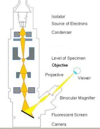
The Transmission Electron Microscope (TEM) was the first type of Electron Microscope to be developed and is patterned exactly on the Light Transmission Microscope except that a focused beam of electrons is used instead of light to examine the specimen. It was developed by Max Knoll and Ernst Ruska in Germany in 1931. The first Scanning Electron Microscope (SEM) debuted in 1942 with the first commercial instruments around 1965. Its late development was due to the electronics involved in "scanning" the beam of electrons across the sample (see Figure 4). |
Figure 4 Types of Microscope |
[view large image] |
 |
The conventional electron microscopy is nowadays called TEM (transmission electron microscopy). The ray of electrons is produced by a pin-shaped cathode heated up by current. The electrons are collected by the anode. The acceleration voltage is between 50 and 150 kV. The higher it is, the shorter are the electron waves and the higher is the power of resolution. But this factor is hardly ever limiting. The power of resolution of electron microscopy is usually restrained by the quality of the lens-systems and especially by the technique with which the preparation has been achieved. Modern gadgets have powers of resolution that range from 0.5 - 10 nm. The useful magnification is therefore more than 1,000,000X. |
Figure 5 TEM |
 |
television techniques. The method is suitable for the depiction of preparations with conductive surfaces. Biological objects have thus to be made conductive by coating with a thin layer of heavy metal (usually gold is taken). The power of resolution is normally smaller than in transmission electron microscopes, but the depth of focus is several orders of magnitude greater. The surface of the object is scanned with the electron beam point by point whereby secondary electrons are set free. The intensity of this secondary radiation is dependent on the angle of inclination of the object's surface. The secondary electrons are collected by a detector that sits at an angle at the side above the object. The signal is then enhanced electronically. The magnification can be chosen smoothly and the image appears a little later on a viewing screen. |
Figure 6 SEM [view large image] |
| Characteristic | Compound Microscope | Transmission E. Microscope | Scanning E. Microscope |
|---|---|---|---|
| Resolution (Average) | 500 nm | 10 nm | 2 nm |
| Resolution (Special) | 100 nm | 0.5 nm | 0.2 nm |
| Magnifying Power | up to 1,500X | up to 5,000,000X | ~ 100,000X |
| Depth of Field | poor | moderate | high |
| Type of Objects | living or non-living | non-living | non-living |
| Preparation Technique | usually simple | skilled | easy |
| Preparation Thickness | rather thick | very thin | variable |
| Specimen Mounting | glass slides | thin films on copper grids | aluminum stubs |
| Field of View | large enough | limited | large |
| Source of Radiation | visible light | electrons | electrons |
| Medium | air | vacuum | vacuum |
| Nature of Lenses | glass | 1 electrostatic + a few em. lenses | 1 electrostatic + a few em. lenses |
| Focusing | mechanical | current in the objective lens coil | current in the objective lens coil |
| Magnification Adjustments | changing objectives | current in the projector lens coil | current in the projector lens coil |
| Specimen Contrast | by light absorption | by electron scattering | by electron scattering |
 |
 |
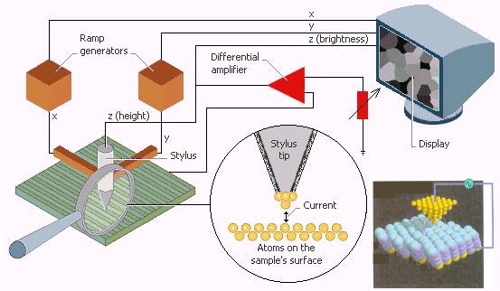
conducting sample (see Figure 7). A STM can resolve images at the atomic level. As the stylus moves across the sample, the current produced is monitored and kept constant to a value set by a gauge (depicted by the arrow in Figure 7). To keep the current constant, the height of the stylus changes as it scans the sample. The display shows the height of the stylus as changes in brightness or color (to represent the third dimension) as the tip is scanned across the display. Figure 8 shows the scanning tunnelling micrograph of gold atoms on a graphite substrate. It displays |
Figure 7 STM |
Figure 8 Gold Atoms [view large image] |
electron clouds surrounding the atomic nuclei, which have high concentration of positive charges. |
 |
 |
The AFM (Atomic Force Microscope, Figure 9) is a slight variation of the STM. Here's a summary of its design: 1. There is a moving cantilever to execute the plotting in the horizontal x-y plane. 2. Force between the tip and the sample lead to a deflection of the cantilever. 3. The deflection is measured by reflection of a laser spot on the top surface of the cantilever into an array of photodiodes. 4. A feedback mechanism is employed to maintain a constant force between the tip-to-sample. The rise and fall of the tip plots the topography of the sample. |
Figure 9 AFM Schematic Diagram [view large image] |
Figure 10 AFM Imaging |
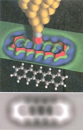
This kind of microscope has been in used since 1986. Recently in 2009, an improvement has been made by placing a carbon monoxide molecule on the tip. Choosing |
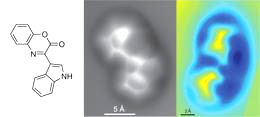 |
An AFM imaging in 2010 shows another organic molecule called cephalandole A taken from deep sea bacteria. The image was captured by placing it on the surface of a salt crystal. Figure 11 shows the chemical formula (as deduced from the imaging), the atomic locations (in middle), and electron density (on the right). Researchers are still debating what these AFM images are really showing. They are also worrying that the structure of |
Figure 11 Molecular Images [view large image] |
the molecule might be altered when it is deposited on the crystal surface. The technique is not going to replace crystallography any time soon. |
 |
 |

|
Figure 12 Phase Shift Interference |
Figure 13 Diffraction [view large image] |
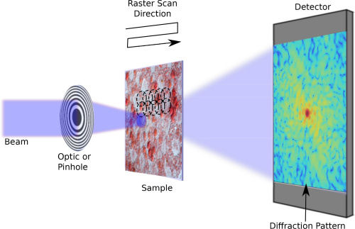
Normal photography relies on the contrast of luminosity (modulus) over the image to show the details. However, for nano-sized or faraway objects subtend very small solid angle, ptychograpy can render details otherwise not shown. |
 |
 |
 to +. to +. |
Figure 14 Ptychography Setup [view large image] |
Figure 15 Modulus and Phase [view large image] |
 |
The ptychographic image is compared with the one taken by the compound microscope in Figure 16. While the ptychography shows clearly the hexagonal pattern of the MoS2 crystal down to a sulfur vacancy (indicated by the red arrow), the bright field photograph could display only a blurring image for |
Figure 16 Ptychographic Image [view large image] |
each hexagon. See "Electron Ptychography of 2D Materials to Deep Sub-angstrom Resolution" for the latest development in 2018. |