

| Home Page | Overview | Site Map | Index | Appendix | Illustration | About | Contact | Update | FAQ |
|
|
|
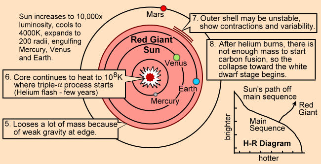
Carbon atoms are made in the Red Giant phase of stellar evolution by the triple alpha process (Figure 01) in the core. Figures 02, 03 depict a series of steps leading up to such stage (also see "Origin of Elements"). Most of the elements in the star are |
Figure 01 Carbon Generation [view large image] |
Figure 02 Red Giant Phase |
Figure 03 Helium Burning [view large image] |
eventually thrust into space by blowing stellar winds or ejected during supernova explosion. |
 |
 |
The nucleus of carbon atom has 6 neutrons (N) and 6 protons (P) with 6 electrons moving around outside - 4 of them are valence, chemically active (the two 1s electrons are inert in a complete shell further inward). At ground state, the configuration is in the form of 1s22s22p2, where the leading numeral is the principle quantum number n, s and p are the orbital quantum numbers with  = 0 and 1 respectively, while the superscripts represent the number of electrons in that particular level (each level, e.g., s or px can accommodate at most two electrons with opposite spin orientation, see Figure 04). = 0 and 1 respectively, while the superscripts represent the number of electrons in that particular level (each level, e.g., s or px can accommodate at most two electrons with opposite spin orientation, see Figure 04).
|
Figure 04 Carbon States [view large image] |
Figure 05 Hybridization of CO2 [view large image] |
Energy of the electrons are determined mainly by n with small variation due to other quantum numbers or via external interaction. For example, combination with other atom(s) will change the energy level and configuration in a process called hybridization. |
 |
 |
The structure of graphene is a two dimensional version of the carbon allotropes (Figure 06). Each individual atom possesses three sp2 orbitals which interact with the other ones in its neighborhood to form covalent sigma bonds; while the 4th orbital maintains a weaker van de Waals pi bond for stacking up the layers to form graphite (Figure 04). In single layer, the electrons in the pi bonds link up together to form valence and conduction bands. The bands at the edge of the sheet make contact with each other in |
Figure 06 Hexagonal Lattice of Graphene [view large image] |
Figure 07 Graphene |
6 points (the Dirac cones) at the boundary of the first Brillouin zone (the hexagon in Figure 07) contributing some weird electronic properties as shown later. |
 = h/p (p is the linear momentum) > 2a, where "a" is the bond length. The electrons inside this zone is described by the Hamiltonian H = p2/2m for free particle with corresponding energy E =
  2k2/2m (Figure 07). Near the boundary of this zone, the electrons moving faster with ~ 2a. The corresponding reciprocal length is k = 2
 / ~ /a, its relationship with the energy becomes H =
  vF(
vF(
 k) and E = vF(kx2 + ky2)1/2
(for 2-D graphene sheet)
k) and E = vF(kx2 + ky2)1/2
(for 2-D graphene sheet)
 |
where vF ~ 108 cm/sec is the velocity of the electron corresponding to the Fermi energy, and the Pauli matrices. Thus, the dependence on k becomes linear instead of quadruple. The deviation is caused by the spin-orbit interaction at such location. It is derived from a phenomenological (empirical) model for spin-orbit coupling. The spin in this case is actually pseudo-spin identified to the valence and conduction bands respectively for spin up and down. Pseudo-spin is a term applicable to all kinds of objects having two different properties, e.g., the iso-spin associated with proton and neutron, ... etc. Comparison of such Hamiltonian H by the massless Dirac (Weyl) equations below shows that it is just the same equation with the speed of light c replaced by vF, where E = c|p| = |p| (for c = 1 in natural unit) :
|
Figure 08 Dirac Cones, Formation |
This superficial resemblance underlies the oft quoted statement that the electron becomes massless in graphene. However, massless particle always moves at the velocity of light (not just vF) according to Special Relativity. |
 |
|
Figure 09 Graphene Properties |
The Young's modulus E is related to the spring constant k by the formula : k = E(A/L) where A and L are the cross-section and length of the object respectively. |
 |
|
Figure 10 Graphene Density of State (DOS) [view large image] |
The "Back Gate Voltage" induces change in the Gate Voltage by an amount approximately equal to the change in the source voltage (Figure 09,c). |
 |
graphene (with defects) and oxygen gas is about 530 K. It combusts at 620 K. Graphene melts into an agglomeration of loosely coupled doubled bonded chains at about 6000 K (see melting point for other allotropes at 3800 K in "Properties of Non-Metallic Solids"). Graphene sheet is thermodynamically unstable if its size is less than about 20 nm. A stable structure requires about 6000 atoms, and it becomes the most stable for layer larger than 24,000 atoms. |
Figure 11 Graphene Oxide (GO) |
Graphene oxide (GO) is an important precursor to graphene and has many promising characteristics itself (Figure 11, also see "Properties and Applications of Graphene Oxide"). Its product of photolysis (by sunlight) could persist for a long time posing certain environmental risk (Figure 09,d). |
 = 3.1416x(1/137) = 0.023 (see "Fine Structure Constant Defines Visual Transparency of Graphene"). The absorption becomes saturated when the input optical intensity is above a threshold value.
 |
At THz range (100 THz - 1 GHz, Figure 12,c) in the presence of a bias magnetic field and three layers of graphene, the left-handed circular polarized light (LCP) is reflected, while the right-handed one is absorbed by the graphene (Figure 12,a). A device has been fabricated with such characteristic in 2016 (see "Graphene THz Isolator"). It is an useful example for protecting the input of certain electro-magnetic wave with special property from interference by other kind of em waves. The additional significance of the design is the currently empty THz frequency range, leaving the potential of the unexploited THz band for Optic Fiber data transmission in the future. Figure 12,b is from another research to simulate the LCP reflection in the 1 THz range (see "Circular Polarization Absorbers with Graphene"). |
Figure 12 Graphene Isolator |
BTW, circular polarized light always changes handedness upon reflection (see "Circular Polarization"), also see "Electromagnetic Spectrum" for another display of the frequency range. |
 |
 |
 |
|
Figure 12a Superconductivity [view large image] and |
Figure 12b Cuprate Doping [view large image] |
Figure 12c Pairing of Opposite Spins |
 |
Theory or laboratory testing may look promising, but it is difficult to translate the idea to industrial level without compromising its properties. It is often said that similar to the "age of plastic" in the 20th century, the 21st century belongs to the graphene, i.e., it would be the "age of graphene". Actually, critical assessment should be conducted to evaluate its impact on the environment (see "Toxicity"). It would be a nightmare to see the globe covered with discarded graphene sheets which are invisible, electrical conductive and have the strength to withstand destruction. |
Figure 12d Age of Graphene [view large image] |
| Application | Comment | Status |
|---|---|---|
| Batteries | Improved performance with the incorporation of graphene | Huawei Prototype (2016) |
| Bio-sensor | Sensitive graphene transistor to detect bio-molecules | Glucose sensor prototype (2015) |
| Catalyst | Speeding up the rate of chemical reactions | Evaluating (2014) |
| Conductive Ink | Electricity conduction on paper and other materials | Available since 2009 |
| Contrast Agents | For MRI imaging | Research report (2013) |
| Coolant additive | Enhancing the thermal conductivity of a base fluid | In development (2013) |
| Data Storage | Million-fold improvement over current hard drives | Research report (2015) |
| Drug Delivery | Used as theranostic probes targeting magnetic, infrared, ... sources | Under investigation (2016) |
| Graphene Filters | Filtering salination, molecules, contamination, unwanted radiation | In various research stages (2017) |
| Graphene Coating | Graphene composites on all kinds of surfaces giving novel functionalities | Limited commercialization (2017) |
| Graphene Quantum Dot (GQD) | With size < 30 nm, for biological, opto-electronics, energy, ... applications | For sale (2017) |
| Lubricant | To replace the traditional graphite | Studied in 2014 |
| Magnetic Sensor | Based on Hall Effect | In lab testing stage (2015) |
| Nanoelectromechanical systems | Nanoscale devices integrating electrical and mechanical functionality (NEMS) | In development (2012) |
| Optical Modulator | Use Fermi level tuning to achieve high modulation speed, large bandwidth | Demonstrated (2011) |
| Photodetector | Superior performance by coupling with silicon quantum dots | Demonstrated (2016) |
| PCR Enhancement | Enhancing accuracy of DNA sequencing with graphene oxide | Investigated (2016) |
| Redox | Controlable reduced/oxidized states via electrical stimulus in GO | Demonstrated (2011) |
| Smart Window | Opaque window turns transparent by applying an electric field | In development (2016) |
| Solar Panel | Graphene Oxide (GO) and other compounds may be the better choice | In various research stages (2017) |
| Spintronics | Used in disk drives, random-access memory, and computer processor | Research report (2015) |
| Supercapacitor | Comparable to current lithium-ion batteries | Demonstrated (2015) |
| Thermoelectrics | Converting heat into electricity | Reported (2015) |
| Tissue Engineering | Improvement of mechanical properties. | Under investigation (2013) |
| Transistors | Replacing silicon in transistors by graphene | Under investigations (2015) |
| Transparent Electrodes | In touch screens (see video), liquid crystal displays, organic photovoltaic cells, and organic light-emitting diodes | Introductory phase (2016) |
| Super-elasticity in Deep Freeze | The elasticity over wide temperature range could make it useful in extreme environments such as outer space. | Research report (2019) |
 |
 |
There are many methods to produce graphene sheets (Figure 13). In the 2012 review article "A roadmap for graphene" only those scalable for industrial use are listed (as shown here in Figure 14,a). This is an excellent review on other aspects of graphene as well. A summary from the review for such production methods is provided below. |
Figure 13 Graphene Production |
Figure 14 Graphene Production, Scalable [view large image] |
 |
|
Figure 15 Graphene Production, LPE [view large image] |
 |
control the (grain) size, ripples, doping level and number of layers, ... This technique has been used to produce transparent conductive coating applications (such as touch screens). The process can be improved by adopting novel technique such as "Plasma-Enhanced CVD (PECVD)", in which the precursor is ionized into plasma, and the substrate can be SiO2/Si (Figure 16,b). |
Figure 16 Graphene Production, CVD and PECVD [view large image] |
 |
contrast of the bilayers (Figure 17,b). Only the transmission electron microscope with magnification up to 5x10⁶X is capable to show the graphene structure in detail (Figure 17,c). See "Electron Microscopes" for a brief introduction of the instruments. |
Figure 17 Graphene Imagings |
 |
|
Figure 18 Raman Spectrum of Graphene [view large image] |
The Raman spectrum of the graphene originates from the vibrational transition of the sp2 carbon atoms (see Figure 06). In addition to identify the presence of graphene, the two or three emission bands (instead of lines for isolated atom) can be used to decipher the number of layers in the substance : |
 |
|
Figure 19 Process for Graphene 2D Band Generation [view large image] |
 |
|
Figure 20 Color Space and TCD |
Similar to the distance defined between two spatial points, the Total Color Difference (TCD)  E*ab between two different colors can be defined in color space (see formula in Figure 20). E*ab between two different colors can be defined in color space (see formula in Figure 20). |
E*ab ~ 0. The TCD becomes large when the substances are not the same (see the scale on the right of Figure 20). In this way we can identify an unknown specimen to a standard substance - the graphene in this case. This method
 |
 |
has been demonstrated for identifying graphene accurately in 2008 (see Figure 21, also "Total Color Difference for Rapid and Accurate Identification of Graphene"). A 2013 update uses contrast difference as shown in Figure 22, in which the numerals indicate the layer numbers while the contrast difference is computed from CD = C - Cs, where C is the contrast of the MoS2 nanosheet and Cs for the SiO2/Si substrate. |
Figure 21 Graphene TCD |
Figure 22 Contrast Difference |
See original article "Rapid and Reliable Thickness Identification of Two Dimensional Nanosheets Using Optical Microscopy". |